 i486
Motherboard · 1995
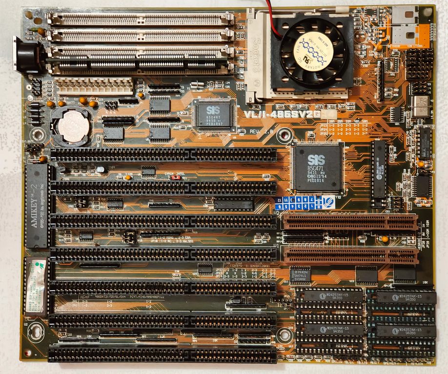
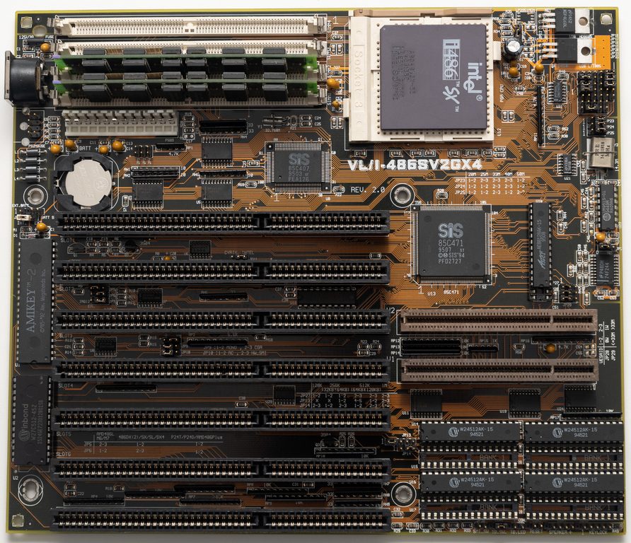
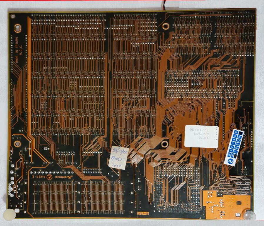
ASUS VL/I-486SV2GX4 REV. 2.1
Works
Details
| Year | 1995 |
| Sockets | Socket 3 (PGA237) |
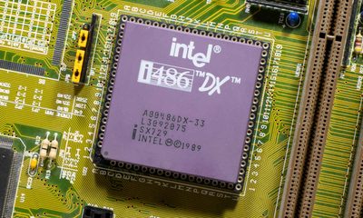
| CPUs | 486 (5V), 486 (3.3V) |
| FSB | 20MHz, 25MHz, 33MHz, 40MHz, 50MHz |
| Chipset | SiS 85C471/407 |
| Form factor | Baby AT |
| L2 cache | 256KB |
| Max RAM | 64MB |
| RAM type | 72-pin FPM |
| PSU connector | AT (6-pin P8 + 6-pin P9) |
| CMOS battery | yes |
| Links | The Retro Web (external) |
Expansion slots & ports
| Slots | |
|---|---|
| ISA 16-bit | 7 |
| VL-Bus | 2 |
| I/O ports | |
|---|---|
| AT keyboard | 1 |
| PS/2 mouse | 1 |
Units
| Unit | Works | State |
|---|---|---|
| ASUS VL/I-486SV2GX4 REV. 2.1(1) | Works | i486 |
| ASUS VL/I-486SV2GX4 REV. 2.1(2) | Broken |
Notes
I have 2 ASUS VL/I-486SV2GX4 REV. 2.1 motherboards, ASUS VL/I-486SV2GX4 REV. 2.1(2) is not working.
Links
The Retro Web has more information about the 2.0 version of the board.
AMD 5X86-133 Notes
Installing an AMD 5X86-133 processor in the VL/I-486SV2GX4 (2.1) motherboard. Had to upgrade the BIOS to 0402 for the BIOS to recognize the CPU properly. Using the recommended jumper settings on the Asus web page, the performance was disappointing (Norton SI(8.0)=188), about the same as Intel DX4). It appears that Asus is setting the processor for write through, even though the AMD 5x86 is a write back. I found that by changing jumper 21 from 2-3 to 3-4 that the Norton SI(8.0) rating goes up to 288! (Equal to a Pentium 90 for a $40 chip!) Everything worked fine except DOS floppy format.
Found the problem. The published ASUS jumper settings for the "hardware trap" don't mention the AMD 5x86. Through experimentation and reading this newsgroup, the problem was solved by having JP5 1-2 and JP6 1-2.
CPU voltage rev2.0
If JP16 is shorted on 1-2, then JP32 sets the voltage. In which case,
- JP32 1-2 = 3.45 V
- JP32 2-3 = 3.6 V
- JP32 OPEN = 4.0 V
If JP16 is OPEN, then the voltage is 5.0 V
Notes
- The BIOS update (SV2G4fix.bin) fixes an issue from the latest BIOS (SV2G4021) in which the system does not properly set register 72h to TAG mode 7+1 when using write-back L2 cache. Without this, write back scores are worse than write through scores. After the BIOS fix, L2 mode write-back cache should be slightly faster than L2 write-through mode.
- A difference between rev 2.0 and rev 2.1 can be found in the jumpers JP31 & JP32 near the CPU Socket
Downloads
| PDFASUS VL/I-486SV2GX4 BIOS Notes 486sv2ggx4-bios-notes.pdf | PDF · 54 KB |
| PDFASUS VL/I-486SV2GX4 REV.2 User Manual asus-vl-i-486sv2gx4-manual-rev2.pdf | PDF · 3.0 MB |
| PDFASUS VL/I-486SV2GX4 REV.2.1 User Manual asus-vl-i-486sv2gx4-manual-rev21.pdf | PDF · 2.3 MB |
| PDFASUS VL/I-486SV2GX4 CPU Jumper Settings CPU Upgrade Jumper Setting for VL_I-486SV2GX4 Motherboard.pdf | PDF · 133 KB |
| PDFASUS VL/I-486SV2GX4 CPU Upgrade Jumper Settings cpu-upgrade-jumper-setting-for-vl-i-486sv2gx4-motherboard.pdf | PDF · 229 KB |
| PDFASUS VL/I-486SV2GX4 Cache Jumper Settings L2 Cache Upgrade and Jumper Setting for VL_I-486SV2G(GX4) Motherboard.pdf | PDF · 105 KB |
| PDFASUS VL/I-486SV2GX4 Jumper Manual rev1.1 MTL Jumper manual (REV. 1.1).pdf | PDF · 338 KB |
Used in