Soyo SY-4SAW
Also known as Soyo SY-4SAW2, Soyo SY-4SAW5 Works
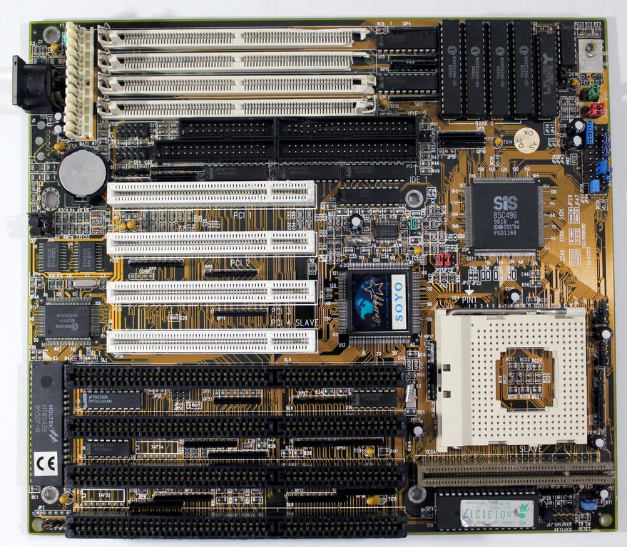
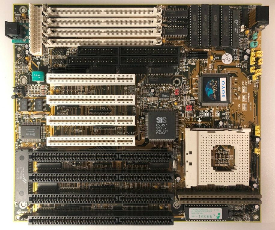
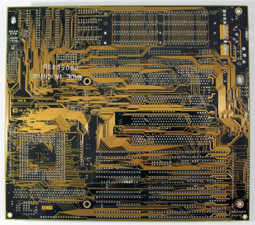
Images from The Retro Web, resized: computerguy096 (CC BY-SA 4.0, 2 images); bjwil1991 (retro-pc_user) (CC BY-SA 4.0)
| Year | 1996 |
| Sockets | Socket 3 (PGA237) |
| CPUs | 486 (3.3V), 486 (5V) |
| FSB | 20MHz, 25MHz, 33MHz, 40MHz, 50MHz |
| Chipset | SiS 85C496/497 |
| Form factor | Baby AT |
| L2 cache | 256KB |
| Max RAM | 256MB |
| RAM type | 72-pin FPM |
| PSU connector | AT (6-pin P8 + 6-pin P9) |
| CMOS battery | yes |
| Links | The Retro Web (external) |
| Slots | |
|---|---|
| ISA 16-bit | 4 |
| VL-Bus | 1 |
| PCI | 4 |
| I/O ports | |
|---|---|
| AT keyboard | 1 |
| Floppy | 1 |
| IDE | 2 |
| PS/2 mouse | 1 |
| Serial | 2 |
| Parallel | 1 |
Memory
The 4SAW doesn't support EDO RAM even though The Retro Web say it does. And SIMM1 slot is the slot closest to the board edge, the reverse of what the jumper manual says.
- Following is probably related to the wrong flash chip type, but BIOS version WA0911 might not work properly, causing the boot to hang at "Updating ESCD", "Building ESCD" or "Verifying DMI Pool Data". In this case, use version WA53. This problem can be probably solved by taking a flash chip which can be written in chunks, like for example SST29EE010.
- Bad or incorrect RAM can lead to BIOS failure; “Award BootBlock Bios v1.0”.
- J15 missing
BIOS
BIOS chip MX 28F1000PPC (MX28F1000P) needs to be programmed with software. We can use Retro Computers/BIOSoftware/BIOS) to flash the BIOS.
Characteristics
Following is a list of notes describing several less-than-obvious features and characteristics of the Soyo SY-4SAW2 486 VIP motherboard. This is a latter-day 486 board based on the SiS 496/497 chipset, notable for PS/2 mouse support and the ability to use just about any CPU compatible with Socket 3.
Most of these characteristics and limitations are a direct consequence of the use of the SiS 85C496/497 chipset and the way said chipset is configured in the 4SAW2 board.
- The VL-Bus slot is target only; an adapter board in this slot cannot work as a bus master. This is a chipset limitation (VL-Bus support is target only). The consequence is that bus-mastering VLB boards such as SCSI adapters won't work, but most graphics cards will.
- PCI slot 4 is slave only; an adapter board in this slot cannot work as a bus master. Again a chipset limitation, although in this case configurable by board designed. The consequences are much the same as above-most PCI graphics cards will work in this slot, but SCSI HBAs or network cards won't. The other three PCI slots do not share this limitation.
- The SIMM1 slot (closest to the board edge) can only use a single side of a memory module. Again a chipset limitation/configuration option. A double-sided SIMM in this slot will typically be detected as one half of its nominal capacity.
- IDE and PCI pins are multiplexed. A chipset limitation-the (VL-Bus) IDE controller pins are shared with PCI address pins on the chipset package, which means that PCI cycles cannot be issued concurrently to IDE cycles. This has a potential performance impact.
- The L2 cache may not be able to cache the entire main memory. This is a chipset limitation-the tag RAM only uses 7 or 8 bits, which limits the number of physical address bits the cache controller can handle. A 256K cache with 7-bit tag can handle 32 MB, with 8-bit tag it's 64 MB. Halving the cache size halves the size of cacheable memory, doubling the cache size doubles it.
- The L2 cache can be interleaved (a chipset design choice). If it is, the cache is somewhat faster. Whether interleaving is used usually depends on the size and type of cache SRAM chips used.
- Main memory access is not interleaved. This is a chipset limitation. As a consequence, memory modules can be mixed in any manner without a performance impact. However, the board may not be as fast as systems with interleaved memory support.
- Although the SiS chipset should support EDO RAM, the board doesn't appear to. This may be a BIOS limitation. The board manual makes no mention of EDO support.
- The turbo switch must be engaged (shorted) for the board to run at full speed.
And one performance note: The SiS chipset's cache controller is relatively slow at handling cache misses. That means most programs which measure main memory speed report very low figures (around 12 MB/s for reads vs approximately 30 MB/s for writes). When L2 cache is disabled, the read speed matches the write speed.. but it's of course still much slower than a cache hit.
Write-Back Enhanced IntelDX4 in the 4SAW2
The board's manual does not describe the jumper settings required for Write-Back Enhanced DX4 processors from Intel. While such processors work when jumpered as regular Intel DX4, the write-back cache will not be utilized (and hence the CPU will in fact behave exactly like a regular DX4).
Contrary to popular belief, the write-back cache on the Intel DX4 is not something software (including firmware/BIOS) can configure. To enable write-back caching, the WB/WT# processor pin must be driven high when the processor is reset. One way to achieve the desired results is jumpering the 4SAW2 board for a P24D processor (Intel DX2 processors with write-back cache) but setting the frequency and voltage jumpers for a DX4 (3.45V).
The way to unambiguously check whether a write-back cache is used or not is a little odd: The processor changes its model number reported through CPUID. The family will be always 4 (for 486), but the model will be 8 for standard DX4 processors and 9 for write-back enhanced DX4 processors with write-back caching in use.
For reference, a 100 MHz Intel DX4 processor shows a score of 197.1 in Norton Utilities 8.0 SYSINFO in the 4SAW2 board. That is true for both a standard DX4 and a write-back enhanced DX4 with standard write-through L1 caching. With write-back cache in use, the same CPU shows a score of 215.0 (slightly better than a 66 MHz Pentium).
Benchmark Results
With the turbo switch engaged, SYSINFO shows a score of 197.1 for a 100MHz Intel DX4 processor, well within the margin of error of the 197.5 score achieved on the Cougar board. Hooray! The rest isn’t quite as bright though, and confirms that the SiS chipset is not that great in terms of performance.
SPEEDSYS now shows video bandwidth as 1946 KB/s which is better than the previous 1392 KB/s but nowhere near the 3771 KB/s with the same card on the Alaris board. This is probably caused by the decoupled SiS 496/497 architecture where the ISA bus is attached to the southbridge, relatively far from the northbridge and the CPU, and behind a “slow link machine”.
Disk performance also increased, from 2.9 MB/s to 3.9 MB/s. Again that’s not as good as the 5.5 MB/s on the Alaris, but it is a sizable improvement. Both the Cougar and the 4SAW2 use a VL-Bus IDE controller and in theory there is no reason why the SiS chipset should be any slower. However, there might be some difference caused by the BIOS (MR BIOS vs. AWARD).
It’s worth mentioning that the SiS 496 northbridge multiplexes the (VLB) IDE pins with the PCI address pins. The consequence of this design is that IDE cycles block PCI cycles and vice versa. This arrangement obviously has a negative performance impact in certain scenarios.
And now for main memory bandwidth: from 9 MB/s reads and 21 MB/s writes, with the turbo switch engaged the performance goes up to 12 MB/s reads and 32 MB/s writes. This is still not quite as good as the 16 MB/s read and 32 MB/s write on the Cougar board, but it’s in the same ballpark.
The L2 cache bandwidth shows a similar story, going from 35 MB/s read and 20 MB/s write to 51 MB/s read and 31 MB/s write, which more or less exactly matches the Alaris board.
| PDF4SAW2 and 4SAW5 USER MANUAL.pdf | PDF · 741 KB |
| PDFMTL Jumper Manual Soyo SY-4SAW-jumpers.pdf | PDF · 488 KB |
| PDFUser Guide & Technical Reference Soyo SY-4SAW.pdf | PDF · 741 KB |